- 您现在的位置:买卖IC网 > Sheet目录3753 > ATMEGA169P-16MCHR (Atmel)MCU AVR 16KB FLASH 16MHZ 64-VQFN
82
8018P–AVR–08/10
ATmega169P
XCK/AIN0/PCINT2 – Port E, Bit 2
XCK, USART External Clock. The Data Direction Register (DDE2) controls whether the clock is
output (DDE2 set) or input (DDE2 cleared). The XCK pin is active only when the USART oper-
ates in synchronous mode.
AIN0 – Analog Comparator Positive input. This pin is directly connected to the positive input of
the Analog Comparator.
PCINT2, Pin Change Interrupt Source 2: The PE2 pin can serve as an external interrupt source.
TXD/PCINT1 – Port E, Bit 1
TXD0, UART0 Transmit pin.
PCINT1, Pin Change Interrupt Source 1: The PE1 pin can serve as an external interrupt source.
RXD/PCINT0 – Port E, Bit 0
RXD, USART Receive pin. Receive Data (Data input pin for the USART). When the USART
Receiver is enabled this pin is configured as an input regardless of the value of DDE0. When the
USART forces this pin to be an input, a logical one in PORTE0 will turn on the internal pull-up.
PCINT0, Pin Change Interrupt Source 0: The PE0 pin can serve as an external interrupt source.
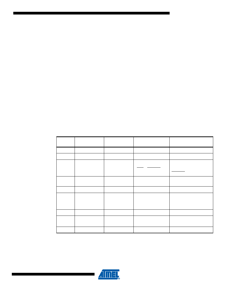
Table 13-16 and Table 13-17 on page 83 relates the alternate functions of Port E to the overrid-
ing signals shown in Figure 13-5 on page 71.
Note:
1. CKOUT is one if the CKOUT Fuse is programmed
Table 13-16. Overriding Signals for Alternate Functions PE7:PE4
Signal
Name
PE7/PCINT7
PE6/DO/
PCINT6
PE5/DI/SDA/
PCINT5
PE4/USCK/SCL/
PCINT4
PUOE
0
USI_TWO-WIRE
PUOV
0
DDOE
CKOUT(1)
0
USI_TWO-WIRE
DDOV
1
0
(SDA + PORTE5)
DDE5
(USI_SCL_HOLD
PORTE4) + DDE4
PVOE
CKOUT(1)
USI_THREE-
WIRE
USI_TWO-WIRE
DDE5
USI_TWO-WIRE DDE4
PVOV
clk
I/O
DO
0
PTOE
–
0
USITC
DIEOE
PCINT7 PCIE0
PCINT6 PCIE0
(PCINT5 PCIE0) +
USISIE
(PCINT4 PCIE0) +
USISIE
DIEOV
1
DI
PCINT7 INPUT
PCINT6 INPUT
DI/SDA INPUT
PCINT5 INPUT
USCKL/SCL INPUT
PCINT4 INPUT
AIO
–
发布紧急采购,3分钟左右您将得到回复。
相关PDF资料
2-1546217-0
TERM BLK RCPT 20POS SIDE 5.08MM
1-1546217-9
TERM BLK RCPT 19POS SIDE 5.08MM
1-1546217-8
TERM BLK RCPT 18POS SIDE 5.08MM
1-1546217-7
TERM BLK RCPT 17POS SIDE 5.08MM
1-1546217-6
TERM BLK RCPT 16POS SIDE 5.08MM
1-1546217-5
TERM BLK RCPT 15POS SIDE 5.08MM
1-1546217-4
TERM BLK RCPT 14POS SIDE 5.08MM
1-1546217-3
TERM BLK RCPT 13POS SIDE 5.08MM
相关代理商/技术参数
ATMEGA169P-16MCU
功能描述:8位微控制器 -MCU AVR 16KB, 512B EE 16MHz 1KB SRAM, 5V
RoHS:否 制造商:Silicon Labs 核心:8051 处理器系列:C8051F39x 数据总线宽度:8 bit 最大时钟频率:50 MHz 程序存储器大小:16 KB 数据 RAM 大小:1 KB 片上 ADC:Yes 工作电源电压:1.8 V to 3.6 V 工作温度范围:- 40 C to + 105 C 封装 / 箱体:QFN-20 安装风格:SMD/SMT
ATMEGA169P-16MU
功能描述:8位微控制器 -MCU AVR 16K FLASH 512B EE 1K SRAM LCD ADC RoHS:否 制造商:Silicon Labs 核心:8051 处理器系列:C8051F39x 数据总线宽度:8 bit 最大时钟频率:50 MHz 程序存储器大小:16 KB 数据 RAM 大小:1 KB 片上 ADC:Yes 工作电源电压:1.8 V to 3.6 V 工作温度范围:- 40 C to + 105 C 封装 / 箱体:QFN-20 安装风格:SMD/SMT
ATMEGA169P-16MU SL383
制造商:Atmel Corporation 功能描述:MCU 8BIT ATMEGA RISC 16KB FLASH 3.3V/5V 64PIN MLF - Tape and Reel
ATMEGA169P-16MUR
功能描述:8位微控制器 -MCU AVR LCD 16KB FLSH EE 512B 1KB SRAM-16MHZ RoHS:否 制造商:Silicon Labs 核心:8051 处理器系列:C8051F39x 数据总线宽度:8 bit 最大时钟频率:50 MHz 程序存储器大小:16 KB 数据 RAM 大小:1 KB 片上 ADC:Yes 工作电源电压:1.8 V to 3.6 V 工作温度范围:- 40 C to + 105 C 封装 / 箱体:QFN-20 安装风格:SMD/SMT
ATMEGA169P-8AU
制造商:ATMEL 制造商全称:ATMEL Corporation 功能描述:Microcontroller with 16K Bytes In-System Programmable Flash
ATMEGA169P-8MU
制造商:ATMEL 制造商全称:ATMEL Corporation 功能描述:Microcontroller with 16K Bytes In-System Programmable Flash
ATMEGA169PA
制造商:ATMEL 制造商全称:ATMEL Corporation 功能描述:8-bit Microcontroller with 16K Bytes In-System Programmable Flash
ATMEGA169PA_1
制造商:ATMEL 制造商全称:ATMEL Corporation 功能描述:High Endurance Non-volatile Memory segments